
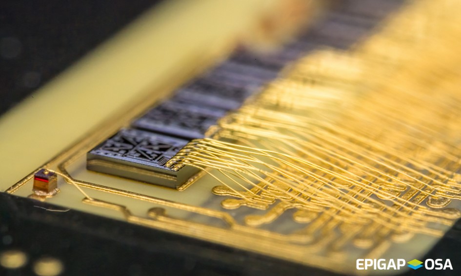
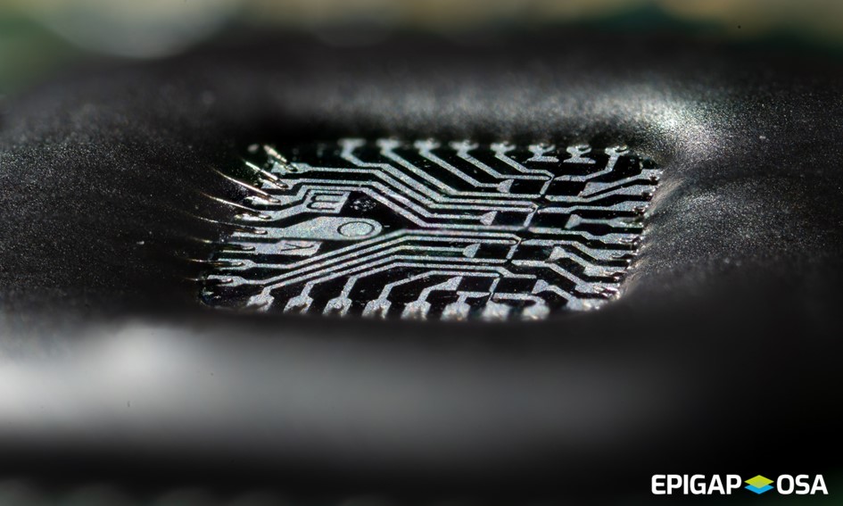
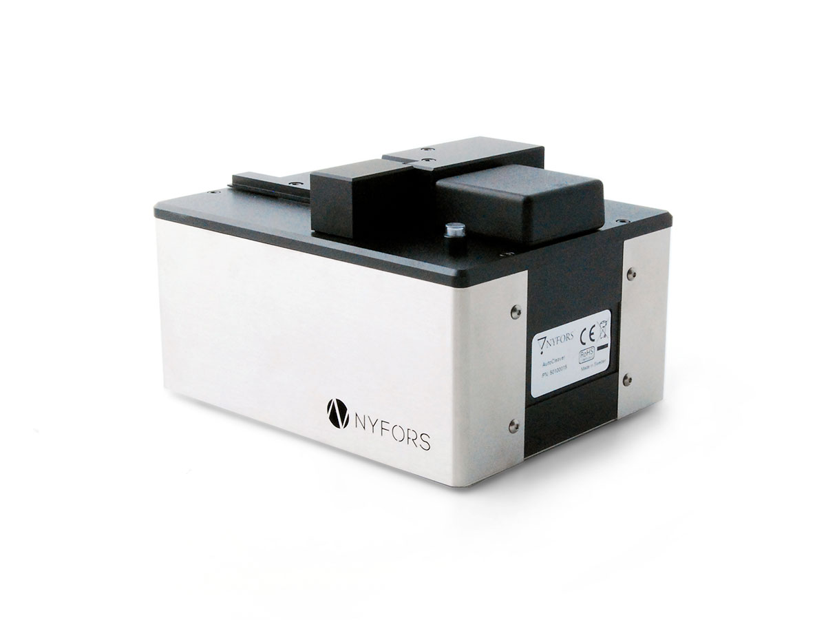
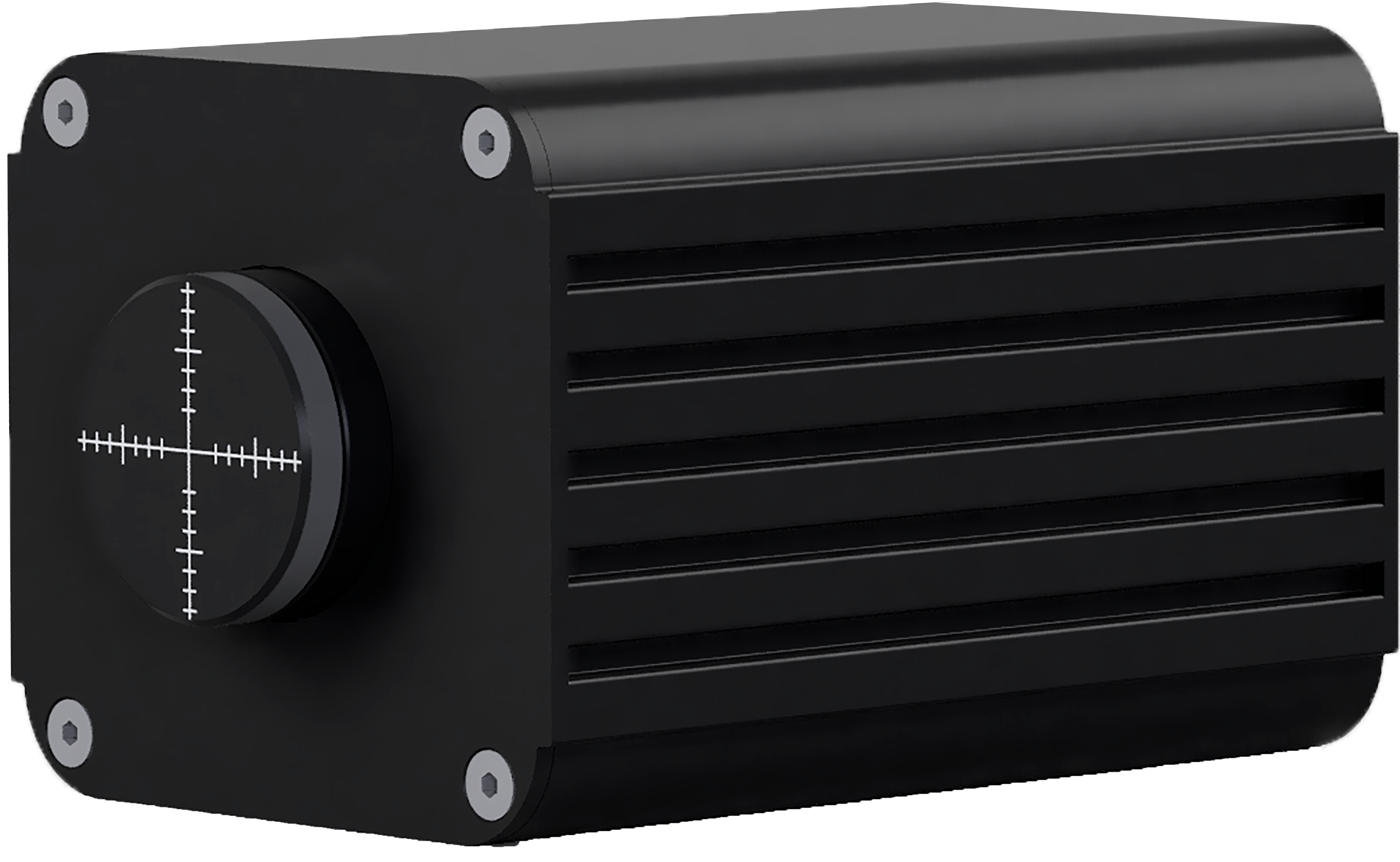
EPIGAP OSA Photonics offers a comprehensive Photonic Assembly service covering the full packaging workflow for optoelectronic components, from individual chip placement to completed hermetically sealed modules. The service supports a wide range of package formats including custom SMD layouts, TO-cans, Chip-on-Board (CoB) assemblies, and multichip modules, with placement accuracy down to +/-10 µm and multichip assemblies integrating 20 or more components per module. All assembly work is performed in-house at the Berlin Kopenick facility under controlled conditions, with complete lot traceability.
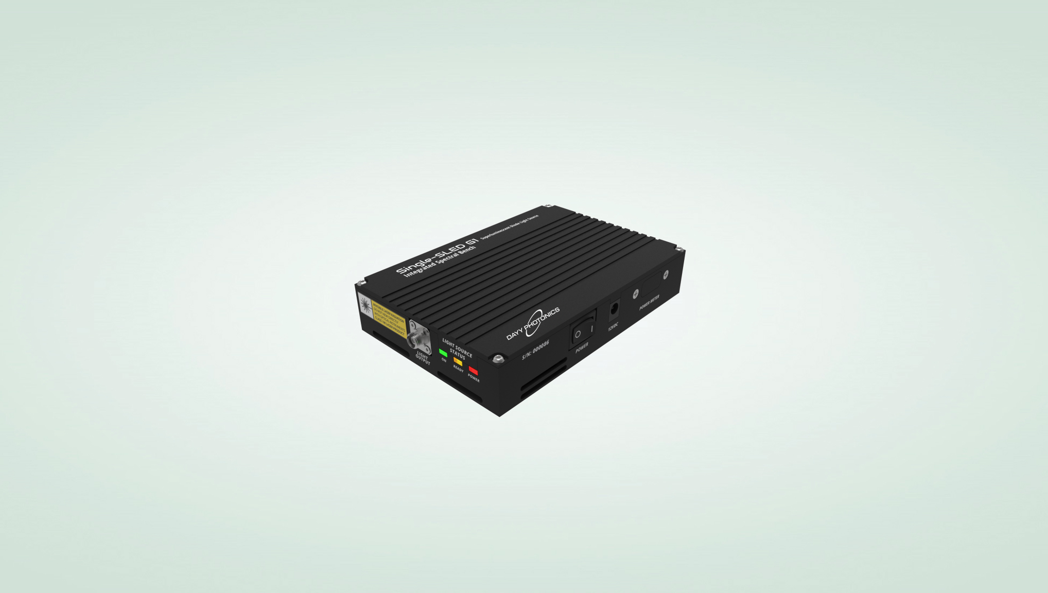
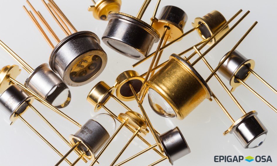
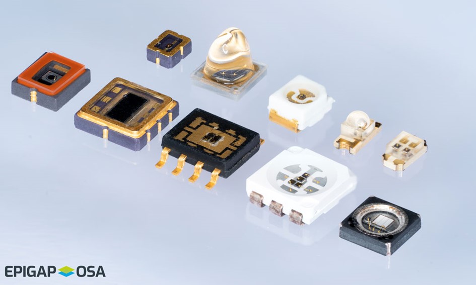
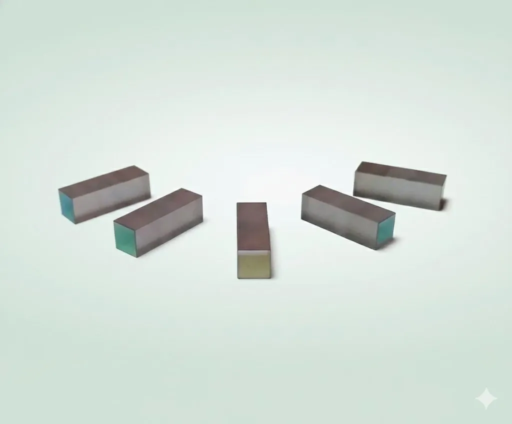
The assembly service is structured around five core capabilities: chip bonding and pick-and-place, gold wire bonding, encapsulation, TO packaging, and SMD packaging. Wire bonding uses gold wire from 17 to 30 µm diameter with ball-wedge and wedge-wedge techniques, qualified by pull and shear testing to MIL standards. Encapsulation options span flat, dam-and-fill, glob top, and lensed formats in clear, white, or light-blocking black materials, with phosphor conversion coatings available for white LED or NIR emission applications. Hermetic TO-cans are assembled under nitrogen or trimix atmosphere, with optional thermoelectric cooling (TEC) integration and custom optical caps including AR coatings and bandpass filters.
This service is especially suited to OEM customers in medical technology and biophotonics, industrial sensor and automation, and safety and security segments who need small-to-medium production series with tight spectral and binning specifications, serialized documentation, and complete supply chain management. EPIGAP OSA handles everything from prototype to series production, including burn-in, qualification, tape-and-reel delivery, and failure analysis.


.png)
.png)


.jpeg)